 | –≠–ª–µ–∫—Ç—Ä–æ–Ω–Ω—ã–π –∫–æ–º–ø–æ–Ω–µ–Ω—Ç: MC1488N | –°–∫–∞—á–∞—Ç—å:  PDF PDF  ZIP ZIP |
MC1488, SN55188, SN75188
QUADRUPLE LINE DRIVERS
SLLS094C - SEPTEMBER 1983 - REVISED MAY 2004
1
POST OFFICE BOX 655303
∑
DALLAS, TEXAS 75265
D
Meet or Exceed the Requirements of ANSI
TIA / EIA-232-E and ITU Recommendation
V.28
D
Current-Limited Output: 10 mA Typical
D
Power-Off Output Impedance: 300
Minimum
D
Slew Rate Control by Load Capacitor
D
Flexible Supply-Voltage Range
D
Input Compatible With Most TTL Circuits
description/ordering information
The MC1488, SN55188, and SN75188 are
monolithic quadruple line drivers designed to
interface data terminal equipment with data
communications equipment in conformance with
ANSI TIA/EIA-232-E, using a diode in series with
each supply-voltage terminal as shown under
typical applications.
The SN55188 is characterized for operation over
the full military temperature range of - 55
∞
C to
125
∞
C. The MC1488 and SN75188 are
characterized for operation from 0
∞
C to 70
∞
C.
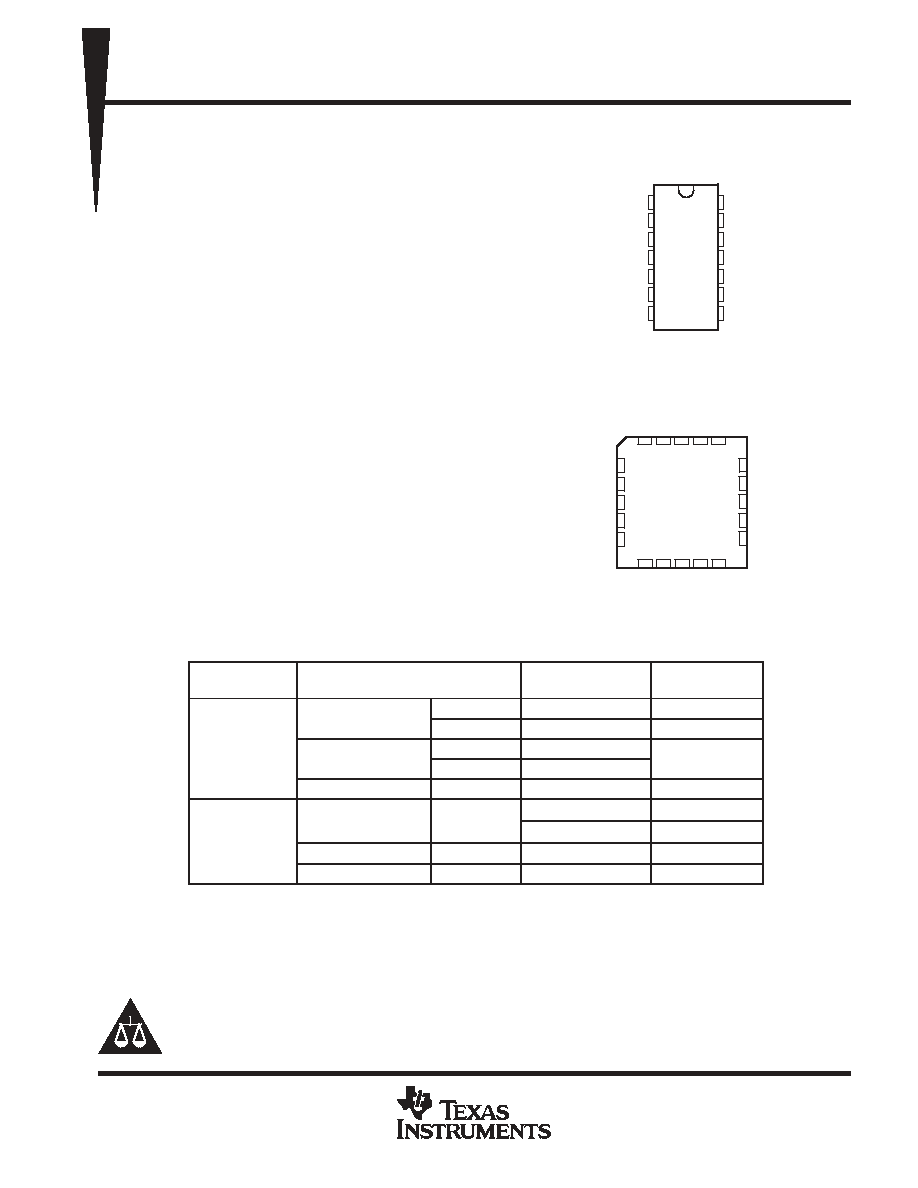
ORDERING INFORMATION
TA
PACKAGE
ORDERABLE
PART NUMBER
TOP-SIDE
MARKING
PDIP (N)
Tube of 25
MC1488N
MC1488N
PDIP (N)
Tube of 25
SN75188N
SN75188N
0
∞
C to 70
∞
C
SOIC (D)
Tube of 50
SN75188D
SN75188
0 C to 70 C
SOIC (D)
Reel of 2500
SN75188DR
SN75188
SOP (NS)
Reel of 2000
SN75188NSR
SN75188
CDIP (J)
Tube of 25
SN55188J
SN55188J
- 55
∞
C to 125
∞
C
CDIP (J)
Tube of 25
SNJ55188J
SNJ55188J
- 55
∞
C to 125
∞
C
CFP (W)
Tube of 150
SNJ55188W
SNJ55188W
LCCC (FK)
Tube of 55
SNJ55188FK
SNJ55188FK
Package drawings, standard packing quantities, thermal data, symbolization, and PCB design guidelines are
available at www.ti.com/sc/package.
Copyright
2004, Texas Instruments Incorporated
PRODUCTION DATA information is current as of publication date.
Products conform to specifications per the terms of Texas Instruments
standard warranty. Production processing does not necessarily include
testing of all parameters.
Please be aware that an important notice concerning availability, standard warranty, and use in critical applications of
Texas Instruments semiconductor products and disclaimers thereto appears at the end of this data sheet.
1
2
3
4
5
6
7
14
13
12
11
10
9
8
V
CC -
1A
1Y
2A
2B
2Y
GND
V
CC +
4B
4A
4Y
3B
3A
3Y
SN55188 . . . J OR W PACKAGE
SN75188 . . . D, N, OR NS PACKAGE
MC1488 . . . N PACKAGE
(TOP VIEW)
3
2
1 20 19
9 10 11 12 13
4
5
6
7
8
18
17
16
15
14
4A
NC
4Y
NC
3B
1Y
NC
2A
NC
2B
SN55188 . . . FK PACKAGE
(TOP VIEW)
1A
NC
3Y
3A
4B
2Y
GND
NC
NC - No internal connection
CC+
V
CC
-
V
On products compliant to MIL PRF 38535, all parameters are tested
unless otherwise noted. On all other products, production
processing does not necessarily include testing of all parameters.
MC1488, SN55188, SN75188
QUADRUPLE LINE DRIVERS
SLLS094C - SEPTEMBER 1983 - REVISED MAY 2004
2
POST OFFICE BOX 655303
∑
DALLAS, TEXAS 75265
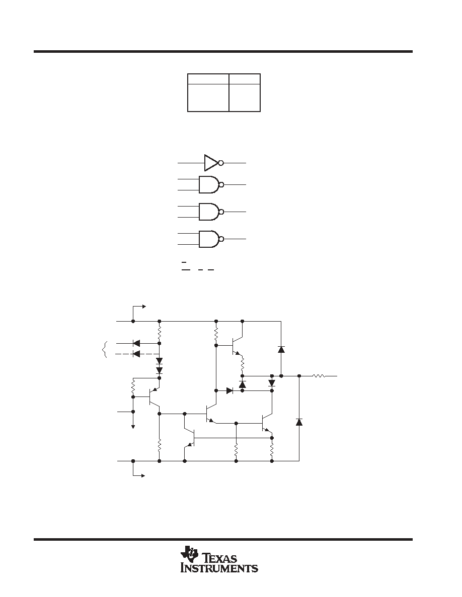
FUNCTION TABLE
(drivers 2-4)
A
B
Y
H
H
L
L
X
H
X
L
H
H = high level, L = low level,
X = irrelevant
logic diagram (positive logic)
9
5
4
2
10
12
13
4Y
3Y
2Y
1Y
1A
2A
2B
3A
3B
4A
4B
11
8
6
3
Positive logic
Y = A (driver 1)
Y = AB or A + B (drivers 2 thru 4)
schematic (each driver)
Output
300
70
3.7 k
10 k
To Other Drivers
VCC -
Drivers
Other
To
GND
3.6 k
Input(s)
B
A
VCC +
70
6.2 k
8.2 k
Drivers
To Other
Resistor values shown are nominal.
MC1488, SN55188, SN75188
QUADRUPLE LINE DRIVERS
SLLS094C - SEPTEMBER 1983 - REVISED MAY 2004
3
POST OFFICE BOX 655303
∑
DALLAS, TEXAS 75265
absolute maximum ratings over operating free-air temperature (unless otherwise noted)
Supply voltage, V
CC +
at (or below) 25
∞
C free-air temperature (see Notes 1 and 2)
15 V
. . . . . . . . . . . . . . . . .
Supply voltage, V
CC -
at (or below) 25
∞
C free-air temperature (see Notes 1 and 2)
-15 V
. . . . . . . . . . . . . . . .
Input voltage, V
I
-15 V to 7 V
. . . . . . . . . . . . . . . . . . . . . . . . . . . . . . . . . . . . . . . . . . . . . . . . . . . . . . . . . . . . . . . . . . . .
Output voltage, V
O
-15 V to 15 V
. . . . . . . . . . . . . . . . . . . . . . . . . . . . . . . . . . . . . . . . . . . . . . . . . . . . . . . . . . . . . . . . .
Continuous total power dissipation (see Note 2)
See Dissipation Rating Table
. . . . . . . . . . . . . . . . . . . . . . . . . .
Package thermal impedance,
JA
(see Notes 3 and 4): D package
86
∞
C/W
. . . . . . . . . . . . . . . . . . . . . . . . . . . .
N package
80
∞
C/W
. . . . . . . . . . . . . . . . . . . . . . . . . . . .
NS package
76
∞
C/W
. . . . . . . . . . . . . . . . . . . . . . . . . . .
Operating virtual junction temperature, T
J
150
∞
C
. . . . . . . . . . . . . . . . . . . . . . . . . . . . . . . . . . . . . . . . . . . . . . . . . . .
Case temperature for 60 seconds, FK package
260
∞
C
. . . . . . . . . . . . . . . . . . . . . . . . . . . . . . . . . . . . . . . . . . . . . .
Lead temperature 1,6 mm (1/16 inch) from case for 60 seconds: J or W package
300
∞
C
. . . . . . . . . . . . . . . .
Storage temperature range, T
stg
-65
∞
C to 150
∞
C
. . . . . . . . . . . . . . . . . . . . . . . . . . . . . . . . . . . . . . . . . . . . . . . . . . .
Stresses beyond those listed under "absolute maximum ratings" may cause permanent damage to the device. These are stress ratings only, and
functional operation of the device at these or any other conditions beyond those indicated under "recommended operating conditions" is not
implied. Exposure to absolute-maximum-rated conditions for extended periods may affect device reliability.
NOTES:
1. All voltage values are with respect to the network ground terminal.
2. For operation above 25
∞
C free-air temperature, refer to the maximum supply voltage curve, Figure 6. In the J package, SN55188
chips are alloy mounted.
3. Maximum power dissipation is a function of TJ(max),
JA, and TA. The maximum allowable power dissipation at any allowable
ambient temperature is PD = (TJ(max) - TA)/
JA. Selecting the maximum of 150
∞
C can affect reliability.
4. The package thermal impedance is calculated in accordance with JESD 51-7.
DISSIPATION RATING TABLE
PACKAGE
TA
25
∞
C
POWER RATING
DERATING FACTOR
ABOVE T = 25 C
TA = 70
∞
C
POWER RATING
TA = 125
∞
C
POWER RATING
PACKAGE
TA
25 C
POWER RATING
DERATING FACTOR
ABOVE TA = 25
∞
C
TA = 70 C
POWER RATING
TA = 125 C
POWER RATING
FK
1375 mW
11.0 mW/
∞
C
880 mW
275 mW
J
1375 mW
11.0 mW/
∞
C
880 mW
275 mW
W
1000 mW
8.0 mW/
∞
C
640 mW
200 mW
recommended operating conditions
SN55188
MC1488, SN75188
UNIT
MIN
NOM
MAX
MIN
NOM
MAX
UNIT
VCC + Supply voltage
7.5
9
15
7.5
9
15
V
VCC - Supply voltage
- 7.5
- 9
- 15
- 7.5
- 9
- 15
V
VIH
High-level input voltage
1.9
1.9
V
VIL
Low-level input voltage
0.8
0.8
V
TA
Operating free-air temperature
- 55
125
0
70
∞
C
MC1488, SN55188, SN75188
QUADRUPLE LINE DRIVERS
SLLS094C - SEPTEMBER 1983 - REVISED MAY 2004
4
POST OFFICE BOX 655303
∑
DALLAS, TEXAS 75265
electrical characteristics over operating free-air temperature range, V
CC
±
=
±
9 V (unless otherwise
noted)
PARAMETER
TEST CONDITIONS
SN55188
MC1488, SN75188
UNIT
PARAMETER
TEST CONDITIONS
MIN
TYP
MAX
MIN
TYP
MAX
UNIT
VCC + = 9 V,
6
7
6
7
VOH
High-level output voltage
VIL = 0.8 V,
VCC + = 9 V,
VCC - = - 9 V
6
7
6
7
V
VOH
High-level output voltage
VIL = 0.8 V,
RL = 3 k
VCC + = 13.2 V,
9
10.5
9
10.5
V
RL = 3 k
VCC + = 13.2 V,
VCC - = - 13.2 V
9
10.5
9
10.5
VCC + = 9 V,
- 7
- 6
- 7
- 6
VOL
Low-level output voltage
VIH = 1.9 V,
VCC + = 9 V,
VCC - = - 9 V
- 7
- 6
- 7
- 6
V
VOL
Low-level output voltage
VIH = 1.9 V,
RL = 3 k
VCC + = 13.2 V,
- 10.5
- 9
- 10.5
- 9
V
RL = 3 k
VCC + = 13.2 V,
VCC - = - 13.2 V
- 10.5
- 9
- 10.5
- 9
IIH
High-level input current
VI = 5 V
10
10
µ
A
IIL
Low-level input current
VI = 0
- 1
- 1.6
- 1
- 1.6
mA
IOS(H)
Short-circuit output
ß
VI = 0.8 V,
VO = 0
- 4.6
- 9
- 13.5
- 6
- 9
- 12
mA
IOS(H)
Short-circuit output
current at high levelß
VI = 0.8 V,
VO = 0
- 4.6
- 9
- 13.5
- 6
- 9
- 12
mA
IOS(L)
Short-circuit output
ß
VI = 1.9 V,
VO = 0
4.6
9
13.5
6
9
12
mA
IOS(L)
Short-circuit output
current at low levelß
VI = 1.9 V,
VO = 0
4.6
9
13.5
6
9
12
mA
ro
Output resistance,
VCC + = 0,
VCC - = 0,
300
300
ro
Output resistance,
power off
VCC + = 0,
VO = - 2 V to 2 V
VCC - = 0,
300
300
VCC + = 9 V,
All inputs at 1.9 V
15
20
15
20
VCC + = 9 V,
No load
All inputs at 0.8 V
4.5
6
4.5
6
ICC +
Supply current from
VCC + = 12 V,
All inputs at 1.9 V
19
25
19
25
mA
ICC +
Supply current from
VCC +
VCC + = 12 V,
No load
All inputs at 0.8 V
5.5
7
5.5
7
mA
VCC +
VCC + = 15 V,
All inputs at 1.9 V
34
34
VCC + = 15 V,
No load, TA = 25
∞
C
All inputs at 0.8 V
12
12
VCC - = - 9 V,
All inputs at 1.9 V
- 13
- 17
- 13
- 17
VCC - = - 9 V,
No load
All inputs at 0.8 V
- 0.5
- 0.015
ICC -
Supply current from ICC -
VCC - = - 12 V,
All inputs at 1.9 V
- 18
- 23
- 18
- 23
mA
ICC -
Supply current from ICC -
VCC - = - 12 V,
No load
All inputs at 0.8 V
- 0.5
- 0.015
mA
VCC - = - 15 V,
All inputs at 1.9 V
- 34
- 34
VCC - = - 15 V,
No load, TA = 25
∞
C
All inputs at 0.8 V
- 2.5
- 2.5
VCC + = 9 V,
VCC - = - 9 V,
333
333
PD
Total power dissipation
VCC + = 9 V,
No load
VCC - = - 9 V,
333
333
mW
PD
Total power dissipation
VCC + = 12 V,
No load
VCC - = - 12 V,
576
576
mW
All typical values are at TA = 25
∞
C.
The algebraic convention, in which the less positive (more negative) limit is designated as minimum, is used in this data sheet for logic voltage
levels only, e.g., if - 6 V is a maximum, the typical value is a more negative voltage.
ß Not more than one output should be shorted at a time.
MC1488, SN55188, SN75188
QUADRUPLE LINE DRIVERS
SLLS094C - SEPTEMBER 1983 - REVISED MAY 2004
5
POST OFFICE BOX 655303
∑
DALLAS, TEXAS 75265
switching characteristics, V
C C
±
=
±
9 V, T
A
= 25
∞
C
PARAMETER
TEST CONDITIONS
MIN
TYP
MAX
UNIT
tPLH
Propagation delay time, low- to high-level output
220
350
ns
tPHL
Propagation delay time, high- to low-level output
RL = 3 k
,
CL = 15 pF,
100
175
ns
tTLH
Transition time, low- to high-level output
RL = 3 k
,
CL = 15 pF,
See Figure 1
55
100
ns
tTHL
Transition time, high- to low-level output
See Figure 1
45
75
ns
tTLH
Transition time, low- to high-level output
RL = 3 k
to 7 k
,
CL = 2500 pF,
2.5
µ
s
tTHL
Transition time, high- to low-level output
RL = 3 k
to 7 k
,
CL = 2500 pF,
See Figure 1
3.0
µ
s
Measured between 10% and 90% points of output waveform
Measured between 3 V and - 3 V points on the output waveform (TIA / EIA-232-E conditions)
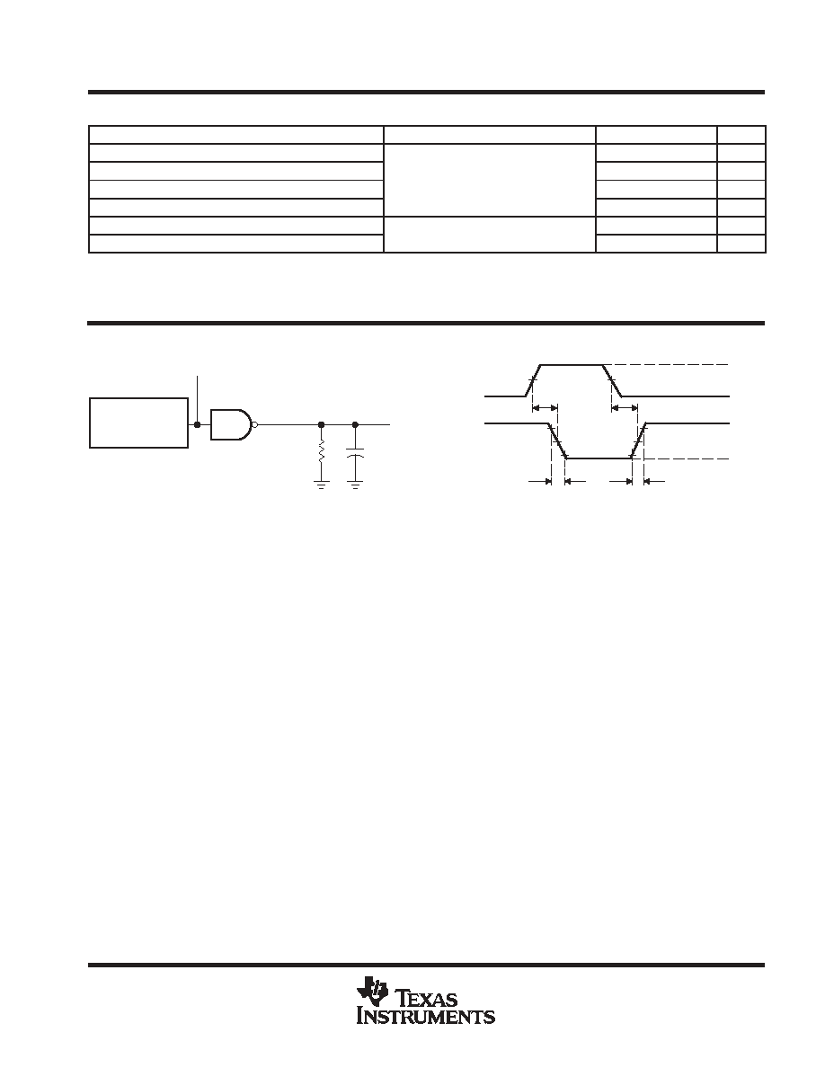
PARAMETER MEASUREMENT INFORMATION
10%
50%
90%
Output
10%
50%
90%
1.5 V
Input
tPHL
tPLH
1.5 V
3 V
0 V
VOH
VOL
tTLH
tTHL
VOLTAGE WAVEFORMS
TEST CIRCUIT
Output
(see Note B)
CL
RL
Input
Pulse
Generator
(see Note A)
NOTES: A. The pulse generator has the following characteristics: tw = 0.5
µ
s, PRR
1 MHz, ZO = 50
.
B. CL includes probe and jig capacitance.
Figure 1. Test Circuit and Voltage Waveforms

MC1488, SN55188, SN75188
QUADRUPLE LINE DRIVERS
SLLS094C - SEPTEMBER 1983 - REVISED MAY 2004
6
POST OFFICE BOX 655303
∑
DALLAS, TEXAS 75265
TYPICAL CHARACTERISTICS
Figure 2
VO - Output V
oltage - V
VOLTAGE TRANSFER CHARACTERISTICS
ŒŒŒŒŒŒŒŒ
ŒŒŒŒŒŒŒŒ
VCC + = 6 V, VCC - = - 6 V
9
6
3
0
- 3
- 6
- 9
1.8
1.6
1.4
1.2
1
0.8
0.6
0.4
0.2
- 12
2
12
0
ŒŒŒŒŒŒŒŒŒ
VCC + = 12 V, VCC - = - 12 V
ŒŒŒŒŒŒŒŒ
ŒŒŒŒŒŒŒŒ
VCC + = 9 V, VCC - = - 9 V
ŒŒŒ
ŒŒŒ
RL = 3 k
TA = 25
∞
C
V
O
VI - Input Voltage - V
Figure 3
IO - Output Current - mA
OUPUT CURRENT
vs
OUTPUT VOLTAGE
Load Line
VOH(VI = 0.8 V)
VCC - = - 9 V
16
12
8
4
0
- 4
- 8
- 12
- 16
12
8
4
0
- 4
- 8
- 12
- 20
16
20
VO - Output Voltage - V
- 16
ŒŒŒŒŒ
VOL(VI = 1.9 V)
ŒŒŒŒ
ŒŒŒŒ
3-k
ŒŒŒŒŒ
ŒŒŒŒŒ
VCC + = 9 V
ŒŒŒŒ
ŒŒŒŒ
TA = 25
∞
C
I O
Figure 4
IOS - Short-Circuit Output Current - mA
SHORT-CIRCUT OUTPUT CURRENT
vs
FREE-AIR TEMPERATURE
IOS(L) (VI = 1.9 V)
ŒŒŒŒ
ŒŒŒŒ
VO = 0
ŒŒŒŒŒ
ŒŒŒŒŒ
VCC - = - 9 V
125
100
75
50
25
0
- 25
- 50
- 75
9
6
3
0
- 3
- 6
- 9
- 12
150
12
TA - Free-Air Temperature -
∞
C
- 100
ŒŒŒŒŒ
ŒŒŒŒŒ
VCC + = 9 V
¡¡
¡¡
I OS
ŒŒŒŒŒŒ
ŒŒŒŒŒŒ
IOS(H) (VI = 0.8 V)
Figure 5
¡¡¡¡
¡¡¡¡
¡¡¡¡
¡¡¡¡
SR - Slew Rate - V/
SLEW RATE
vs
LOAD CAPACITANCE
ŒŒŒŒŒ
ŒŒŒŒŒ
TA = 25
∞
C
RL =
VCC - = - 9 V
VCC + = 9 V
100
10
1000
100
1
10000
1000
CL - Load Capacitance - pF
10
µ
s
Data for temperatures below 0
∞
C and above 70
∞
C are applicable to SN55188 circuit only.
MC1488, SN55188, SN75188
QUADRUPLE LINE DRIVERS
SLLS094C - SEPTEMBER 1983 - REVISED MAY 2004
7
POST OFFICE BOX 655303
∑
DALLAS, TEXAS 75265
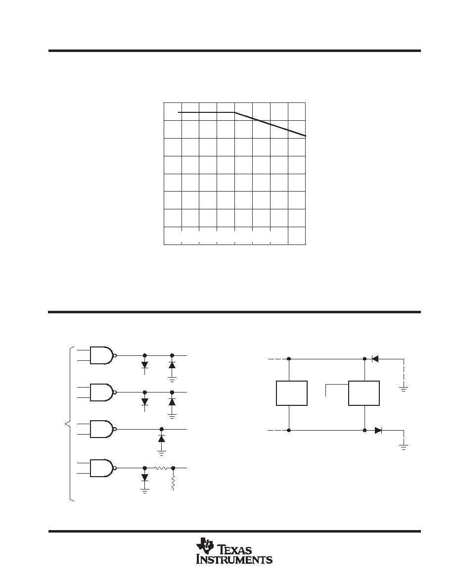
THERMAL INFORMATION
- Maximum Supply V
oltage - V
MAXIMUM SUPPLY VOLTAGE
vs
FREE-AIR TEMPERATURE
RL
3 k
(from each output to GND)
14
12
10
8
6
4
2
100
75
50
25
0
- 25
- 50
0
125
16
TA - Free-Air Temperature -
∞
C
- 75
CC
V
Figure 6
Data for temperatures below 0
∞
C and above 70
∞
C are applicable to the SN55188 circuit only.
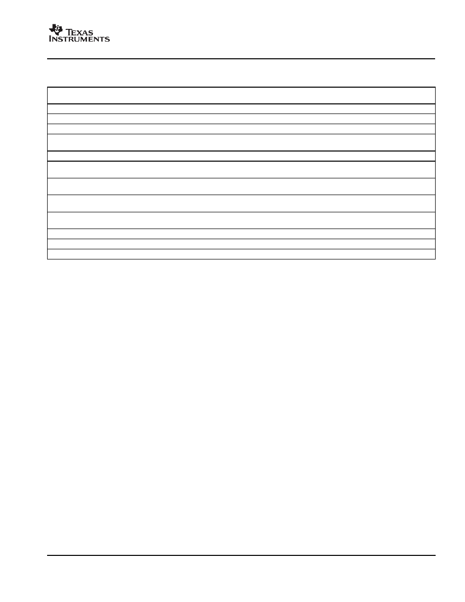
APPLICATION INFORMATION
Diodes placed in series with the VCC+ and VCC - leads protect
the SN55188/SN75188 in the fault condition in which the device
outputs are shorted to
±
15 V, and the power supplies are at low
voltage and provide low-impedance paths to ground.
VCC +
VCC -
±
15 V
Output
VCC +
VCC -
'188
'188
10 k
1 k
- 10 V to 0 V
Output to MOS
or SN75188
1/4 SN55188
- 0.7 V to 10 V
Output to HNIL
1/4 SN55188
or SN75188
- 0.7 V to 5.7 V
Output to DTL
5 V
1/4 SN55188
or SN75188
or SN75188
1/4 SN55188
- 0.7 V to 3.7 V
Output to RTL
3 V
- 12 V
VCC + = 12 V
VCC - = - 12 V
Input From
TTL
or DTL
Figure 7. Logic Translator Applications
Figure 8. Power-Supply Protection to Meet
Power-Off Fault Conditions of
ANSI TIA / EIA-232-E
PACKAGING INFORMATION
Orderable Device
Status
(1)
Package
Type
Package
Drawing
Pins Package
Qty
Eco Plan
(2)
Lead/Ball Finish
MSL Peak Temp
(3)
5962-86889012A
ACTIVE
LCCC
FK
20
1
None
POST-PLATE
Level-NC-NC-NC
5962-8688901CA
ACTIVE
CDIP
J
14
1
None
A42 SNPB
Level-NC-NC-NC
5962-8688901DA
ACTIVE
CFP
W
14
1
None
A42 SNPB
Level-NC-NC-NC
MC1488N
ACTIVE
PDIP
N
14
25
Pb-Free
(RoHS)
CU NIPDAU
Level-NC-NC-NC
SN55188J
ACTIVE
CDIP
J
14
1
None
A42 SNPB
Level-NC-NC-NC
SN75188D
ACTIVE
SOIC
D
14
50
Pb-Free
(RoHS)
CU NIPDAU
Level-2-260C-1 YEAR/
Level-1-235C-UNLIM
SN75188DR
ACTIVE
SOIC
D
14
2500
Pb-Free
(RoHS)
CU NIPDAU
Level-2-260C-1 YEAR/
Level-1-235C-UNLIM
SN75188N
ACTIVE
PDIP
N
14
25
Pb-Free
(RoHS)
CU NIPDAU
Level-NC-NC-NC
SN75188NSR
ACTIVE
SO
NS
14
2000
Pb-Free
(RoHS)
CU NIPDAU
Level-2-260C-1 YEAR/
Level-1-235C-UNLIM
SNJ55188FK
ACTIVE
LCCC
FK
20
1
None
POST-PLATE
Level-NC-NC-NC
SNJ55188J
ACTIVE
CDIP
J
14
1
None
A42 SNPB
Level-NC-NC-NC
SNJ55188W
ACTIVE
CFP
W
14
1
None
A42 SNPB
Level-NC-NC-NC
(1)
The marketing status values are defined as follows:
ACTIVE: Product device recommended for new designs.
LIFEBUY: TI has announced that the device will be discontinued, and a lifetime-buy period is in effect.
NRND: Not recommended for new designs. Device is in production to support existing customers, but TI does not recommend using this part in
a new design.
PREVIEW: Device has been announced but is not in production. Samples may or may not be available.
OBSOLETE: TI has discontinued the production of the device.
(2)
Eco Plan - May not be currently available - please check
http://www.ti.com/productcontent
for the latest availability information and additional
product content details.
None: Not yet available Lead (Pb-Free).
Pb-Free (RoHS): TI's terms "Lead-Free" or "Pb-Free" mean semiconductor products that are compatible with the current RoHS requirements
for all 6 substances, including the requirement that lead not exceed 0.1% by weight in homogeneous materials. Where designed to be soldered
at high temperatures, TI Pb-Free products are suitable for use in specified lead-free processes.
Green (RoHS & no Sb/Br): TI defines "Green" to mean "Pb-Free" and in addition, uses package materials that do not contain halogens,
including bromine (Br) or antimony (Sb) above 0.1% of total product weight.
(3)
MSL, Peak Temp. -- The Moisture Sensitivity Level rating according to the JEDECindustry standard classifications, and peak solder
temperature.
Important Information and Disclaimer:The information provided on this page represents TI's knowledge and belief as of the date that it is
provided. TI bases its knowledge and belief on information provided by third parties, and makes no representation or warranty as to the
accuracy of such information. Efforts are underway to better integrate information from third parties. TI has taken and continues to take
reasonable steps to provide representative and accurate information but may not have conducted destructive testing or chemical analysis on
incoming materials and chemicals. TI and TI suppliers consider certain information to be proprietary, and thus CAS numbers and other limited
information may not be available for release.
In no event shall TI's liability arising out of such information exceed the total purchase price of the TI part(s) at issue in this document sold by TI
to Customer on an annual basis.
PACKAGE OPTION ADDENDUM
www.ti.com
4-Mar-2005
Addendum-Page 1

MECHANICAL DATA
MLCC006B ≠ OCTOBER 1996
POST OFFICE BOX 655303
∑
DALLAS, TEXAS 75265
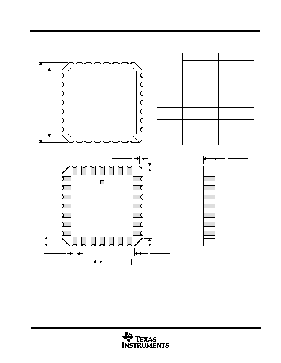
FK (S-CQCC-N**)
LEADLESS CERAMIC CHIP CARRIER
4040140 / D 10/96
28 TERMINAL SHOWN
B
0.358
(9,09)
MAX
(11,63)
0.560
(14,22)
0.560
0.458
0.858
(21,8)
1.063
(27,0)
(14,22)
A
NO. OF
MIN
MAX
0.358
0.660
0.761
0.458
0.342
(8,69)
MIN
(11,23)
(16,26)
0.640
0.739
0.442
(9,09)
(11,63)
(16,76)
0.962
1.165
(23,83)
0.938
(28,99)
1.141
(24,43)
(29,59)
(19,32)
(18,78)
**
20
28
52
44
68
84
0.020 (0,51)
TERMINALS
0.080 (2,03)
0.064 (1,63)
(7,80)
0.307
(10,31)
0.406
(12,58)
0.495
(12,58)
0.495
(21,6)
0.850
(26,6)
1.047
0.045 (1,14)
0.045 (1,14)
0.035 (0,89)
0.035 (0,89)
0.010 (0,25)
12
13
14
15
16
18
17
11
10
8
9
7
5
4
3
2
0.020 (0,51)
0.010 (0,25)
6
1
28
26
27
19
21
B SQ
A SQ
22
23
24
25
20
0.055 (1,40)
0.045 (1,14)
0.028 (0,71)
0.022 (0,54)
0.050 (1,27)
NOTES: A. All linear dimensions are in inches (millimeters).
B. This drawing is subject to change without notice.
C. This package can be hermetically sealed with a metal lid.
D. The terminals are gold plated.
E. Falls within JEDEC MS-004


IMPORTANT NOTICE
Texas Instruments Incorporated and its subsidiaries (TI) reserve the right to make corrections, modifications,
enhancements, improvements, and other changes to its products and services at any time and to discontinue
any product or service without notice. Customers should obtain the latest relevant information before placing
orders and should verify that such information is current and complete. All products are sold subject to TI's terms
and conditions of sale supplied at the time of order acknowledgment.
TI warrants performance of its hardware products to the specifications applicable at the time of sale in
accordance with TI's standard warranty. Testing and other quality control techniques are used to the extent TI
deems necessary to support this warranty. Except where mandated by government requirements, testing of all
parameters of each product is not necessarily performed.
TI assumes no liability for applications assistance or customer product design. Customers are responsible for
their products and applications using TI components. To minimize the risks associated with customer products
and applications, customers should provide adequate design and operating safeguards.
TI does not warrant or represent that any license, either express or implied, is granted under any TI patent right,
copyright, mask work right, or other TI intellectual property right relating to any combination, machine, or process
in which TI products or services are used. Information published by TI regarding third-party products or services
does not constitute a license from TI to use such products or services or a warranty or endorsement thereof.
Use of such information may require a license from a third party under the patents or other intellectual property
of the third party, or a license from TI under the patents or other intellectual property of TI.
Reproduction of information in TI data books or data sheets is permissible only if reproduction is without
alteration and is accompanied by all associated warranties, conditions, limitations, and notices. Reproduction
of this information with alteration is an unfair and deceptive business practice. TI is not responsible or liable for
such altered documentation.
Resale of TI products or services with statements different from or beyond the parameters stated by TI for that
product or service voids all express and any implied warranties for the associated TI product or service and
is an unfair and deceptive business practice. TI is not responsible or liable for any such statements.
Following are URLs where you can obtain information on other Texas Instruments products and application
solutions:
Products
Applications
Amplifiers
amplifier.ti.com
Audio
www.ti.com/audio
Data Converters
dataconverter.ti.com
Automotive
www.ti.com/automotive
DSP
dsp.ti.com
Broadband
www.ti.com/broadband
Interface
interface.ti.com
Digital Control
www.ti.com/digitalcontrol
Logic
logic.ti.com
Military
www.ti.com/military
Power Mgmt
power.ti.com
Optical Networking
www.ti.com/opticalnetwork
Microcontrollers
microcontroller.ti.com
Security
www.ti.com/security
Telephony
www.ti.com/telephony
Video & Imaging
www.ti.com/video
Wireless
www.ti.com/wireless
Mailing Address:
Texas Instruments
Post Office Box 655303 Dallas, Texas 75265
Copyright
2005, Texas Instruments Incorporated